当前位置:
X-MOL 学术
›
ACS Energy Lett.
›
论文详情
Our official English website, www.x-mol.net, welcomes your
feedback! (Note: you will need to create a separate account there.)
Defect Engineering to Achieve Photostable Wide Bandgap Metal Halide Perovskites
ACS Energy Letters ( IF 19.3 ) Pub Date : 2023-05-31 , DOI: 10.1021/acsenergylett.3c00610
Samuele Martani 1 , Yang Zhou 1 , Isabella Poli 1 , Ece Aktas 2 , Daniele Meggiolaro 3 , Jesús Jiménez-López 1 , E Laine Wong 1 , Luca Gregori 3, 4 , Mirko Prato 5 , Diego Di Girolamo 2 , Antonio Abate 2 , Filippo De Angelis 3, 4, 6, 7 , Annamaria Petrozza 1
Affiliation
|
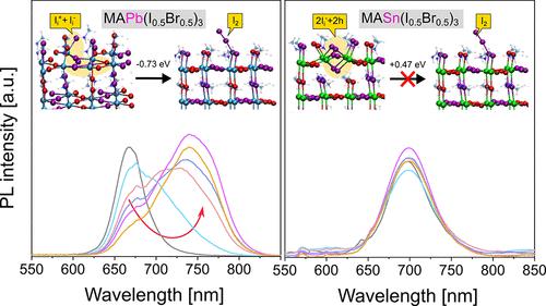
Bandgap tuning is a crucial characteristic of metal-halide perovskites, with benchmark lead-iodide compounds having a bandgap of 1.6 eV. To increase the bandgap up to 2.0 eV, a straightforward strategy is to partially substitute iodide with bromide in so-called mixed-halide lead perovskites. Such compounds are prone, however, to light-induced halide segregation resulting in bandgap instability, which limits their application in tandem solar cells and a variety of optoelectronic devices. Crystallinity improvement and surface passivation strategies can effectively slow down, but not completely stop, such light-induced instability. Here we identify the defects and the intragap electronic states that trigger the material transformation and bandgap shift. Based on such knowledge, we engineer the perovskite band edge energetics by replacing lead with tin and radically deactivate the photoactivity of such defects. This leads to metal halide perovskites with a photostable bandgap over a wide spectral range and associated solar cells with photostable open circuit voltages.
中文翻译:

缺陷工程实现光稳定宽带隙金属卤化物钙钛矿
带隙调谐是金属卤化物钙钛矿的一个重要特性,基准碘化铅化合物的带隙为 1.6 eV。为了将带隙提高到 2.0 eV,一个简单的策略是在所谓的混合卤化物铅钙钛矿中用溴化物部分替代碘化物。然而,此类化合物容易发生光诱导卤化物偏析,导致带隙不稳定,这限制了它们在串联太阳能电池和各种光电器件中的应用。结晶度改进和表面钝化策略可以有效减缓但不能完全阻止这种光引起的不稳定性。在这里,我们确定了触发材料转变和带隙偏移的缺陷和带隙内电子态。基于这些知识,我们通过用锡代替铅来设计钙钛矿带边缘能量学,并从根本上使此类缺陷的光活性失活。这导致金属卤化物钙钛矿在很宽的光谱范围内具有光稳定的带隙,并且相关的太阳能电池具有光稳定的开路电压。
更新日期:2023-05-31
中文翻译:
缺陷工程实现光稳定宽带隙金属卤化物钙钛矿
带隙调谐是金属卤化物钙钛矿的一个重要特性,基准碘化铅化合物的带隙为 1.6 eV。为了将带隙提高到 2.0 eV,一个简单的策略是在所谓的混合卤化物铅钙钛矿中用溴化物部分替代碘化物。然而,此类化合物容易发生光诱导卤化物偏析,导致带隙不稳定,这限制了它们在串联太阳能电池和各种光电器件中的应用。结晶度改进和表面钝化策略可以有效减缓但不能完全阻止这种光引起的不稳定性。在这里,我们确定了触发材料转变和带隙偏移的缺陷和带隙内电子态。基于这些知识,我们通过用锡代替铅来设计钙钛矿带边缘能量学,并从根本上使此类缺陷的光活性失活。这导致金属卤化物钙钛矿在很宽的光谱范围内具有光稳定的带隙,并且相关的太阳能电池具有光稳定的开路电压。


 京公网安备 11010802027423号